Minimizing PCB assembly costs in electronic manufacturing is very important for competitive success. This requires a balance of design complexity with a cost optimization size, number of layers, and material without compromise.
Utilizing sophisticated design software to avoid expensive revisions is also the key to reduce PCB design costs. This article explores an effective strategy on how to reduce PCB design costs, emphasizing the need for careful innovation and planning to achieve quality results in cost reduction.
Strategic optimization of PCB design, which focuses on parameters such as the width of the track, distance, through size, surface layer, and copper weight, can cause a significant reduction in costs in the PCB design without sacrificing quality.
Understand the cost of PCB design
Before answering how you optimize the PCB design, you must understand what makes the PCB costs. Determinants of key costs include:
Board size/complexity
To reduce the cost of PCB design effectively, you must choose a standard board size and simple geometric shape. This strategy minimizes the complexity of production and maximizes manufacturing efficiency, which leads to significant cost savings.
Waiting time
Shortening waiting time increases cash flow and operational efficiency by reducing inventory loads. Effective strategies include closely coordinating with producers for lean production and choosing suppliers known for fast settlement time, optimizing costs and time.
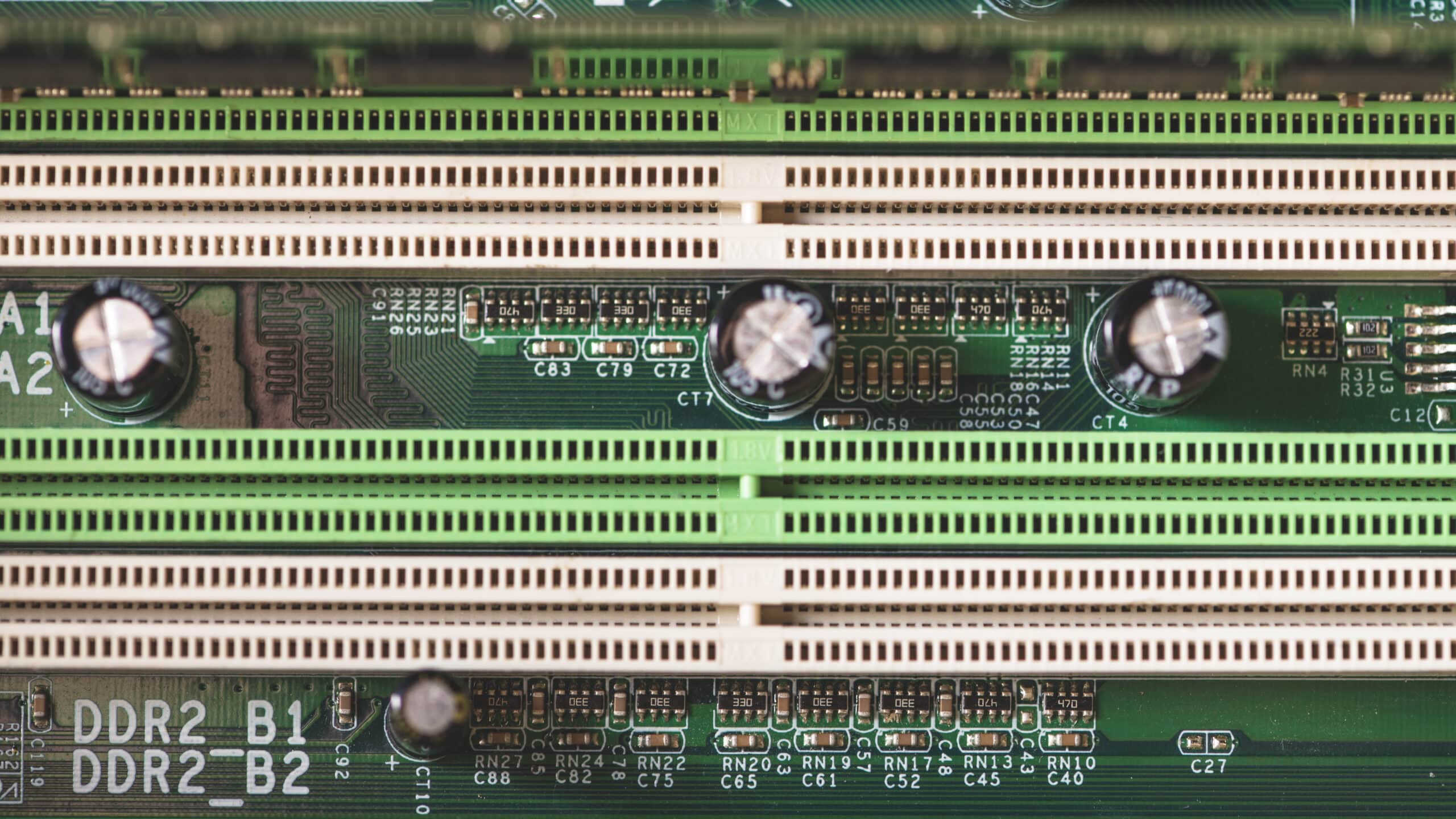
Layer
Minimizing the number of layers in PCB design is very important for cost control, because each additional layer increases fabrication costs. An efficient design requires balance the need for layers of costs, choosing a multilayer configuration only if needed for the complexity of the circuit. This approach not only reduces costs but also simplifies manufacturing, increasing reliability.
Raw material
Choosing appropriate raw materials is very important to control costs. Balancing material performance, endurance, and cost is the key. A slender design and bulk purchase can reduce material costs, create a cost -effective and reliable PCB design.
Final surface
Options such as Hasl, Tin, and OSP are economical and maintain the ability of solder while protecting copper surfaces. Effective cost management involves the selection of the final outcome that balances costs with performance, ensuring PCB’s integrity and functionality without excessive expenditure for simple designs.
Sizes and counts of drill holes
Managing PCB design costs effectively involves optimizing the size of the drill hole and count. Using a larger drill hole if possible and reduce the total number of holes simplify fabrication and cut costs. Avoiding unnecessary small holes and carelessly adjusting drill specifications for economical but functional PCB designs is important.
Mount Surface Technology (SMT)
SMT reduces the size of the board and streamlins the assembly with the placement of efficient components and the layout of a higher density, thereby reducing material costs. The automatic also accelerates production and reduces labor costs, increasing the efficiency of the overall cost of PCB manufacturing.
Filling Vias
Designers must choose a standard size and optimize the distance to control costs. While Vias filled increases structural integrity and thermal management, its use must be balanced with additional costs, ensuring they are only employed when performance benefits justify costs.
Add-on
Emphasizing simplicity in components and design and using bulk orders and standard services helps achieve significant savings. In addition, remain aware of external factors such as exchange rates and material costs are very important for cost-effective designs.
Manufacturer’s choice
Choosing the right PCB manufacturer is very important for cost management. Effective strategies include comparing prices, negotiating volume discounts, and selecting standard board specifications to reduce costs.
Effective design strategy for cost reduction
We have developed an effective design strategy that can help you reduce PCB engineering costs.
Surface installation technology through holes
Turning to Surface Mount Technology (SMT) from traditional methods through holes is the main strategy for reducing PCB design costs. SMT allows the layout of board that is denser and denser and more dense and automatic assembly, reduce the use of materials and accelerate production.
This makes the preferred selected SMT among PCB designers who are aware of the cost for efficiency and potential to reduce costs per unit.
Space Assessment and Array Design
Increasing the efficiency of surface installation technology costs, careful space assessment, and array design in the PCB layout optimizing the use of board space and reducing material costs. Making strategic material choices and evaluation processes ensure that performance needs are met economically.
Layered through the Vias hole
Using a layered through a hole (PTH) VIAS is a cost -effective approach in PCB design, offering savings compared to priciers through options. Balancing its size and functionality correctly and selecting an annular ring uniform and optimal hole size helps minimize costs.
Avoiding the filled VIAS also reduces costs, which leads to cost -effective and functional sound design.
Cost -effective material
Choosing a cost -effective material is very important to reduce the cost of PCB design. It is important to choose materials that balance performance and costs well and consider factors such as batch size, exchange rates, and tariffs.
Choosing the right component, either through a hole or surface installation, also helps streamline costs, ensure efficient and durable PCB fabrication.
Adjust trail and permit requirements
Adjusting the width of the tracks and specifications of the permit is the key for a cost -effective PCB design. By complying with industrial standards and adjusting these parameters to certain design needs, you can minimize the use of materials and simplify manufacturing.
Collaborated with assemblers for strategic adjustments to ensure the design maintains functional integrity and cost efficiency, potentially reducing board size and material costs.
Future trend in PCB design
PCB design trends for 2024 focus on sustainability, ability to adapt to new technology, and efficiency:
- Sustainability: Emphasis on environmentally friendly manufacturing, highlighted by innovations such as water -soluble PCB.
- IoT Adaptation: PCB is being designed to accommodate the increase in the needs of the IoT market, focus on smaller, denser and more flexible products.
- Flexibility with PCB Flex: There is an increase in the use of flexible PCBs in various industries despite the cost challenges due to unique manufacturing needs.
- 3D printing: Gain popularity in PCB manufacturing because of its flexibility in design, cost effectiveness, and environmental benefits.
- High density interconnection PCB: PCB HDI is important for modern electronics because of its improved ability and compatibility for compact devices.
- 5G Technology: PCB design developed to support the demands of 5G technology, focus on smaller, lighter, and thinner designs.
- Artificial intelligence: The effect of AI is to form a PCB design to be stronger, reliable, and can be adjusted to AI and Machine Learning applications.
Conclusion
By mastering techniques such as utilizing volume discounts, choosing strategic partners, and strictly complying with the best design practice, designers can balance economic and functional goals, ensure cost -effective fabrication.
As technology develops, sustainable innovations in this design technique will further increase the efficiency and effectiveness of the cost of making the PCB.
football News
Berita Olahraga
News
Berita Terkini
Berita Terbaru
Berita Teknologi
Seputar Teknologi
Drama Korea
Resep Masakan
Pendidikan
Berita Terbaru
Berita Terbaru
Berita Terbaru


